For some time I have an Agilent 6627A quad power supply, which had one bad channel (the reason I could get it for a good price). While so far I didn't really need it, it always bugged me to have faulty equipment.
The symptom is that the output is always at 0 Volts. The channel is in unregulated state, but otherwise there is no error, it passes self test. The self test mostly covers the digital part only, so this is not a surprise.
I have verified that the readback works by forcing voltage and current on the output. This supply can also sink current, so no harm in doing this.
The channel boards are quite complex, with their own microcontroller, DACs, ADCs, etc, so debugging is far from straightforward.
In this unit channel 1 is bad, which is the lower left board. After some visual inspection for anything suspicious I decided to swap this with channel 2, which is one of the upper boards. This would give better access and I wouldn't have to poke around the line input at the back. So I did that, quite easy, just had to remove 4 screws and a some connectors. Probably this will require re-calibration, but I would do that anyway later.
For initial troubleshooting I went with the guide in the service manual, it has an extensive troubleshooting section. All voltages were ok, the DACs are ok, and the usual suspects were quickly eliminated.
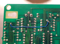
I finally reached Q319, a simple 2N2222A transistor which had a short. Replaced, but nothing happened. I realized that its emitter should be at -7V, but it was not.There was no connection between the -7V regulator and Q319, so I began to trace the connection and saw that the the trace is burned up at one point, so clearly there was some catastrophic event. Maybe it was caused by the shorted transistor or maybe the short happened as a result of something else. Anyway, it needs to be fixed to continue.
Fortunately there were two nearby vias, where i could attach the wire, so it was quickly fixed.
That fixed, the result is that the channel is now jumping between CV, CC and unreg modes and the -7V rail is down to about about -4V.My approach is now to study the schematics in more detail to more deeply understand how it is working and trying to come up with what faults can cause these symptoms.
Stay tuned for the next part, while I continue finding the problem and writing Part 2 of this post.


No comments:
Post a Comment