Sunday, October 3, 2021

Repair of an HP 5334B counter - Part 1 - first looks

Some time ago, I got an HP 5334B counter off eBay. It was advertised az not powering up and it had a best offer option. I like not powering up stuff, as usually they have some simple problems. It was missing the display cover, but since the unit had the OCXO option and based on the pictures I was able to confirm that the HP 10811 oven oscillator was there, I submitted an offer of about the third of what the OCXO is worth by itself. Somewhat to my surprise the offer was accepted and the counter was on its way to me.


Initial inspection has shown that there were no major parts missing and it indeed had the oven oscillator.


After making sure on the line voltage setting, I also confirmed that it did not power up, not even the standby led, which should indicate that the oven is powered up. So I checked the trivial stuff first. The fuse seemed to be good, but I always measure if it does not look obviously blown.


Hmmmm. That OL on the meter is sure makes me suspicious that the fuse is not as good as it looks. I got a replacement and look, it powers up. That sure is easy. Or maybe not, still need to test it.


In case you are wondering in the meantime I was able to get a front panel for a couple of bucks, complete with the display cover. The cover was installed, it simply pops into place and I now have a bunch of replacement switches for vintage HP equipment. It also had the plastic trim on the upper side of the front, so test equipment OCD was avoided this time, by not missing anything from the unit.

However, not all is nice. The trigger led for channel A is always lit and channel A does not work at all. B and C do. Fortunately for someone who repairs test equipment for fun, it was not simply a blown fuse.

So let's get the service manual and follow the signal path for the input. In this case, the gameplan is to simply follow along and see where the signal disappears. The input may have been blown by overvoltage or anything like that could have happened, so a systematic fault finding is the best way to go.

Connecting A and B with the Com key will make Channel B count the A input, but that does not help a lot, since the Common switch as very near to the front of Channel A, only the AC/DC coupling switch (relay) and the 50 ohm input terminating resistor is there. But, at least we know that those are good.

On the other hand I discovered that R113 is fried. So there was very likely some overload situation.


The only problem is that R113 is in Channel B, so this is not the cause of a faulty Channel A.

In the next part I'll go trough the testing of Channel A components. 

Thursday, May 20, 2021

Repairing an Agilent 6627A quad power supply - Part 1

For some time I have an Agilent 6627A quad power supply, which had one bad channel (the reason I could get it for a good price). While so far I didn't really need it, it always bugged me to have faulty equipment.

The symptom is that the output is always at 0 Volts. The channel is in unregulated state, but otherwise there is no error, it passes self test. The self test mostly covers the digital part only, so this is not a surprise.

I have verified that the readback works by forcing voltage and current on the output. This supply can also sink current, so no harm in doing this.

The power supply has 3 main components. A huge (I mean huge!) transformer, as this is a linear supply. A control board + front panel and the channel boards. In this case it has 4 identical (nearly, as for packaging reasons they are 2 + 2 more or less symmetric boards. In other configuration there are less channels and there are double sized boards with double power. But the 6627A has 4 40W 0-50V output boards. This can greatly simplify debugging as there is a working reference.
The whole setup is in a quite clever fold out design, where the upper output boards fold out on a hinged aluminium plate.

The channel boards are quite complex, with their own microcontroller, DACs, ADCs, etc, so debugging is far from straightforward.

In this unit channel 1 is bad, which is the lower left board. After some visual inspection for anything suspicious I decided to swap this with channel 2, which is one of the upper boards. This would give better access and I wouldn't have to poke around the line input at the back. So I did that, quite easy, just had to remove 4 screws and a some connectors. Probably this will require re-calibration, but I would do that anyway later. 

For initial troubleshooting I went with the guide in the service manual, it has an extensive troubleshooting section. All voltages were ok, the DACs are ok, and the usual suspects were quickly eliminated. 

I finally reached Q319, a simple 2N2222A transistor which had a short. Replaced, but nothing happened. I realized that its emitter should be at -7V, but it was not.

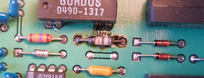
There was no connection between the -7V regulator and Q319, so I began to trace the connection and saw that the the trace is burned up at one point, so clearly there was some catastrophic event.  Maybe it was caused by the shorted transistor or maybe the short happened as a result of something else. Anyway, it needs to be fixed to continue.

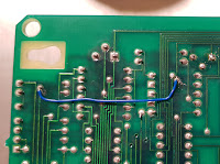
The trace broke where it passes between the two pins. The solution is to bridge this. Since it is at a very inconvenient place, I decided to use a jumper wire on the solder side instead.  

Fortunately there were two nearby vias, where i could attach the wire, so it was quickly fixed.

That fixed, the result is that the channel is now jumping between CV, CC and unreg modes and the -7V rail is down to about about -4V.
So obviously there are still things remaining to be fixed.

My approach is now to study the schematics in more detail to more deeply understand how it is working and trying to come up with what faults can cause these symptoms.

Stay tuned for the next part, while I continue finding the problem and writing Part 2 of this post.


Tuesday, April 20, 2021

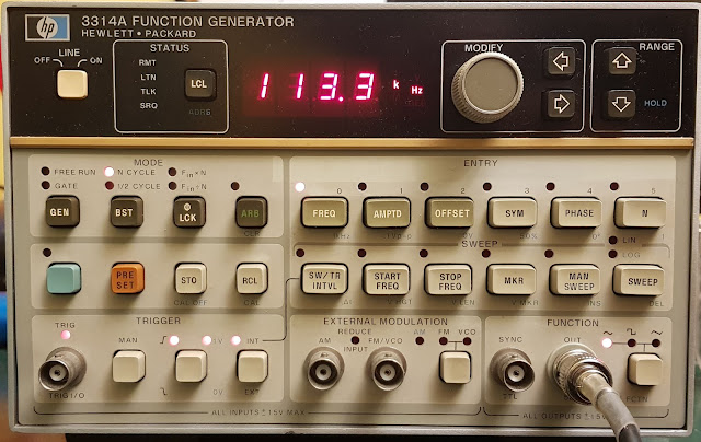
Fixing an HP 3314A function generator - repair complete!

Wrapping up from Part 2

I managed to source a CA3082 locally, so there is no need for any workaround. I popped it in, and it worked.


I had a problem with one of the reed relays, but this time it was not on the driver side, but on the actual reed contact. It wouldn't work however I exercised it by quick switching. By luck, I had a handful of reed contacts with the same size, so I snipped the old one out, it was spot welded and soldered in the new one. Carefully, they are fragile. I say this from experience.

 Fortunately both leads could be soldered well, it would have been hard to weld them again. 

I went trough the adjustment section of the manual, got everything in spec. Now I have proudly resurrected a vintage 3314A from a quite bad repair attempt by a previous owner. 

It is a nice and still quite capable instrument.


Tuesday, April 13, 2021

Fixing an HP 3314A function generator - Part 2.

Continuing with the repair of the HP 3314A function generator that was "repaired" by a previous owner. I left off at the decision of checking everything that was done to it.

First I had to clean up. 5 of the 6 EPROM adapter boards were soldered into the instrument and for some unknown reason 1 was in a socket. I started beeping out the connection between the EPROMs for the data and address lines, and sure enough, found several where there were no connection. Not very surprising, given what I have seen with the 74S74 IC in the clock generator circuit. Also, some of the adapter boards were bad, there was no connection between some of the pins, there were cold solder joins there.

Very carefully I started removing the adapters. Even though HP made quite sturdy PCBs, I didn't want to risk any more damage, so I snipped the pins of the adapters and removed them one by one. I also removed the two 74ls373, they are the ones with the two jumpers next to them. You can see the solder blobs at their ends near to the EPROMs. That is where their pins were snipped and soldered from above, presumably to fit after the adapter boards were already put in.

Once everything was removed, I was already able to see four broken traces under U209, the one in the socket. Those were fixed with scraping off the solder mask and soldering twin wires there.

Then I checked for continuity for every pad related to the ROMs and installed high quality sockets and replaced the 2 74ls373. All this took quite some time, but was well worth the effort as at the end I had a nice board.

I again double checked continuity to the sockets and proceeded with getting the EPROMs fixed.

Next, I turned my attention to the adapter boards. My initial idea was to scrap the 6 EPROMs and just use one with a 74ls148 priority encoder figuring out the additional address lines from the 6 chip select signals. But to make it nice it needed some PCB, and work, and then I also realized I actually had 3 of the same (well, nearly same, they were blue, and a bit different layout) adapter boards from an earlier project, so I actually only had to clean up three of the old ones. So I went with tidying up those boards, as the previous owner even got those wrong, instead of using the proper jumper places he used bodge wires to configure it. After some tedious work with the solder sucker and the iron, I got all six EPROMs ready for action.

Plugged them in and did again a quick check that everything is in place and turned the instrument on. It started the countdown and then did the calibration sequence without problem. Honestly I wasn't expecting that, I was prepared to see a bunch of calibration errors at best.

Halleluja! But does it play Halleluja? No! There is no output. There is output from the sync, but nothing from the signal. 

Ok, don't panic, just think. If the calibration sequence is successful, then there must be a signal with proper amplitude and frequency where the calibration signal is picked off. Looking at the schematics, this is done nearly at the very end, after the output amplifier, but before the output attenuator.  I quickly verified this with a scope. Looks like the signal is lost somewhere at the reed relays. So the main suspect now is the relays themselves or the drivers of the relay coils.

The relays are controlled by a latch which in turn controls a CA3082 transistor array. The latch seems to be good, but the voltages on some of the outputs of the array were strange. As a quick test I piggybacked some random NPN transistor on one of these outputs, and surprise surprise, the corresponding relay came to life. 

So the CA3082 seems to be a fault. This is an obsolete part, not too easy to get. Of course I made a purchase on eBay for some cheap solution, I'm pretty much certain that it will be fake, but let's take some chances. As plan B I also designed a small PCB with surface mount transistors as a pin compatible replacement. 
So right now I'm waiting for either a working replacement or the PCB. This will take a couple of weeks probably. Hopefully this will fix the instrument. I'll write a Part 3. of this post once this happens.


Monday, April 12, 2021

Fixing an HP 3314A function generator - Part 1

 Some time ago I scored a nice looking HP 3314A function generator of eBay. It was advertised as not powering up, so there was a chance that there is some simple problem. I took a chance and was able to get it for cheap.

When it arrived, I took a closer look. I immediately noticed something rattling inside, and this is what I saw after I had opened it up.


One of the EPROMs was loose and bouncing around inside the case. I first though that it may be that simple, but a closer look provided a much gloomier forecast. The EPROMs were infact in a small adapter boards, so someone has been here before. The adapter boards by themselves are not a problem, the Mostek ROMs in these units are known to fail and can quite easily be replaced by 2764 EPROMs, using an adapter to fix the pinout differences.

However, the soldering job on these adapters were horrible. There were large blobs of solder everywhere, sockets being melted, bodge wires going over and under sockets, etc. So I was not too optimistic, when I reseated the EPROM. Especially that I noticed that two EPROMs had some of their pins crushed when they were apparently misaligned during insertion. See pin 19 of U208 in the above picture. Someone was very careless in the past. I fixed those, fortunately without breaking the bent pins.

Flipping the power switch, the fan starts, but no sign of life. Not even the ROM checksum test.

OK, lets dig deeper. First the trivial stuff. Power rails were good, all within spec with voltage and ripple. Next, check the CPU activity. Ooops! Out of the two clock signals, only one is there, that can't be good.

Let's go and follow the signal path for the clock. The two-phase clock is derived from the master crystal oscillator and I very quickly discovered that  the problem is at a 74S74 IC. Interestingly enough, this IC is in a socket, so looks like someone replaced it at some point of time in the past. Hmmm. Anyway, because of the socket, I was quickly able to replace it, without any effect.

It was time to examine the board more carefully. I removed it from the clever fold out metal sheet, and this is what I saw.

The previous owner had butchered the PCB for the U201, the 74s74. (I'm not sure what he was using, a flamethrower and some blacksmith tools maybe.) Anyway a trace was broken at one of the pins and replaced with a jumper wire. Which became pinched under one of the screws holding down the board and got grounded. No wonder the clock was a flat-liner. I guess this worked for some time while the insulation got chewed up, or the screw was finally tightened, so this is why the previous repairer did not notice it.

I redid the soldering and patched the trace, so got rid of the long wire. Immediately I had nice clock, but still no sign of life. 

Next step is Signature Analysis (SA). Some like it, some don't, but HP was very keen on having this debug function in their CPU driven instruments. In my experience it can be a very useful and easy to use tool for some of the troubleshooting steps. I hooked up my Sony-Tektronix 308 Data Analyzer to go trough the  SA tests. I still had a feeling that the ROMs would be the problems, but let's exclude everything else first. 

The first test is the freerun test, when the CPU is fed a harmless instruction at every memory read to just sweep trough all the memory addresses. So we are basically supposed to see A15-A0 count up to cover the whole 64k memory range. With the SA this will also test most of the memory decoder functions. 

The first attempt wasn't successful. The signatures on the CPU pins checked out fine, but two of the address lines after the 74LS373 latches were bad. I looked at then with a scope and looked like the two lines were shorted. Obviously the prime suspects were the 373s. Even more so, as there were huge blobs of solder on some of the pins on the component side. Looks like that someone wanted to replace them after the EPROM adapter cards were soldered in and they prevented from lifting the 373 out of the PCB and also inserting the new one. So he cut the offending pins flush with the bottom of the IC and then soldered them in from above. Which of course resulted in a short. Then probably at this time he gave up, and put the unit on eBay, where I got it.

I fixed the short, and then the freerun SA tests finally completed successfully. But still no sign of operation. Next came the ROM SA tests, which basically do a checksum like test on the EPROMs. 

3 out of 6 ROMs were good, the rest did not give a stable reading. But by wiggling the ROMS, sometimes I got a good result. Obviously the excellent soldering skills of the previous owner struck again.

At this point I decided to remove all the ROMs, check the EPROM contents, check the adapter cards and check the PCB under the ROMs, as I felt that if the previous owner did such a massacre with a 14 pin IC, then a 24 pin would not be any better. And boy,  I was right.

Stay tuned for the next part.

Monday, March 8, 2021

Readout for the 5S14N

Introduction

The 5S14N is a very versatile sampling plugin for the Tektronix 5000 series scope. While some say it is the little brother of the 7S14 for the 7000 series mainframes, it is actually the other way around. The 7S14 contains the same board as the 5S14N, so far that it actually has the 5000 series edge connector on them, but unused, having an adapter board to connect to the mainframe. The only feature missing from the 5S14N is the readout capability, hence the N suffix.

The slower, 5000 series mainframes do not have readout, but the faster 5400 series do. Since I have a 5440, I started wondering if it would be possible to add the readout, as the way the readout works is exactly the same as in the 7000 series scopes. BTW, the readout is masterpiece of analog engineering, created by Barrie Gilbert of Gilbert cell fame.

After consulting with the service manual, it seemed like a viable idea. Since both plugins are practically the same, except for the mainframe interface, I was hoping that Tek did not produce two version with only a few components missing. There is the readout board, which contains the resistors to program the currents for the mainframe readout circuitry, which is not in the 5S14N, but that didn't seem to be a problem, as that could easily be duplicated. However, if the switch contacts from the timebase or the input attenuators are missing, then there is not a lot of hope. After taking apart the unit and doing some measurements, it turned out that fortunately this is not the case. Everything is there that is needed for the readout. Well, nearly everything, these are the missing components:

  • The readout board
  • Interconnect between the readout and the horizontal board
  • Interconnect between the readout and the vertical switch board
  • Connecting harness between the readout board and the input attenuator switches
  • Connection between the readout board and the mainframe interface

So, let's go trough these items and see what can be done.

The readout board

The readout board is a fairly simple circuit, consisting mostly of resistors, that create the programming currents for the readout in the mainframe. The resistors are switched by the cam switches of the horizontal timebase, the vertical attenuator switches and some other switch, like Ch2 invert, etc.
Additionally, there are some active components to implement the 10x/1x probe readout switching and the readout enable for the enabled channels.
Due to the excellent service manuals from the time this plugin was produced, the schematics are given in the 7S14 manual. Fortunately, the same mechanical implementation can be used, as the board is fastened to the casing of the delay line, which is also the same in the 7S14 and the 5S14N, there is no need to figure out where to put the extra board. Given all this, my approach was very simple: make a copy of the boards.

I used KiCad for the whole process. First, I entered the schematics into ESchema basically copying the one in the service manual. 


The components are simple, the resitors must have the same value as on the schematic, as they control the currents for the readout. For the diodes, the usual 1N4148 or any similar diode is ok.

Substitutes had to be found for the transistors. For Q1 and Q2 I used MPSA14 NPN Darlingtons. Q3 and Q4 PF5101 N jFETs and for Q5 and Q6 2N2222 NPN transistors.

Q5 and 6 have to have Uce above 30 v and Q3 and 4 have to have UGS above 30 V. The later is especially critical, as a lot of jFETs has this voltage lower, they will break down and possibly blow the readout current switch in the scope. There are a lot of devices that may be used, just make sure, you get the pinout right on the PCB, or change the design to suit.

Then design the PCB. The placements of the components are in the service manual, but the layout is not, or at least was not readable in my copy. So I basically used the same placement of the components and then designed the layout myself. There is nothing critical in there and it is simple enough to easily implement on a double sided board, even without using vias.


Once done, it was sent to JLCPCB for manufacturing, and after some time, I had a very nice PCB.
The KiCAD project and Gerber files are available at https://github.com/szigix/5S14N-readout

Interconnect for the horizontal board

This is easy. The horizontal board has the pin headers already populated for the readout so all I needed were a couple pieces of ribbon cable with pin header socket on each end. Unfortunately I did not have the crimp connectors used by Tektronix, so I simply soldered pin header sockets at the end of the cables. I made them a bit longer than what is really necessary, so it would be easier to assemble.

Interconnect for the vertical board

This is similar to the horizontal board, some ribbon cables with socket at the end. Not too easy to plug them into the vertical switch board, but long tweezers and sharp eyes can help.

The only exception is P4 on the readout board, which goes to P4-1 and P6-3 on the horizontal board. Those headers already have connectors on them, but the one pin missing. I found some crimp connector sockets that I was able to insert into the connector housing and used that. All other connectors go to the vertical switch board, which is hard to access, but otherwise pose no problem.

Be careful not to mix P3 and P4 they are both two pin connectors next to each other. Mixing them may blow Q5 and Q6.
 

Attenuator connection

This one is a fiddly job. We need the connection from the attenuator switches, uncal switches and Ch2 invert switch to the readout board. Very very fortunately, the the rotary switches for the attenuators contain the wafer and contacts for the readout. Without them, it would be probably pretty much impossible to retrofit readout. The same is true for the Variable pots, they do have the switches for the uncal indicator, just unconnected. So the task was to figure out what goes where and then how to connect.

The switches are hard to access, but by removing the fastener nuts from the switches and from the gain and the time diff pots, they can be wiggled out to access the connections. I soldered wires to them and after some switching back and forth and checking with a continuity tester I was able to find the pinout. The diagram shows what goes where. The pin names are referencing the names on the 7S14 schematics of the readout board. Looking at the wafer closer to the front of the instrument, there are five solder tabs, two of them are actually between the attenuator resistors. The pin for 2 and 5 are close to each other, so this positively identifies the whole setup. The switches for the two channels are in different orientation when in place, but the pinout is the same.
The "uncal" switches and the Ch 2 invert pushbutton are trivial. 6 wires come from Ch1 and 7 (because of invert) from Ch2. I laced the wires and soldered the connectors onto the other end.

This is the  connection for the wiring. P1 on the readout board is for Ch2:

P1-1 - col
P1-2 - 0
P1-3 - 00
P1-4 - 2
P1-5 - 5
P1-6 - uncal (<)
P1-7 - invert

P2 is for Ch1, be careful, this is not the same pinout:

P2-1 - uncal (<)
P2-2 - 5
P2-3 - 2
P2-4 - 00
P2-5 - 0
P2-6 -col 

This picture shows Ch2 already wired and the wires laced up, see the blue, red, white, green, brown wires soldered to the front wafer. Also, observ the blue wire (col) going to the Ch2 invert switch. Ch1 is still to go, some of the trimmers are removed from the front panel to provide access to the switch. 


The mainframe interface

This is easy, but not very elegant. Fortunately the fingers on the edge connector are there, but they are not connected to anything, just the bare pads. I wish Tektronix had put at least a solder pad next to them. So the solution is to simply solder the wire at the inner end of the connector, bodge wire style. That should do it. Once everything is tested, I will probably put a dab of epoxy there to mechanically stabilize the wires. Be careful no to pinch the wires when the frame holding the rear of the modules are put back.

Fortunately, there are holes that can conveniently be used to access the other side of the connector.

This is how the edge connectors are connected. The first 3 columns show the function of the pin, where Ch1c is Ch1 column current, Ch1r is row current and TS1 is TimeSlot pulse number 1, etc. 
The next two columns show where these are connected on the horizontal boards and the last two on the vertical boards. 10-1 means pin 1 of P10 of the readout board, except the two with the *, where these are connected to P4 of the vertical switch board.
 
Number  A  B     HorizB    Vert A  B
24   Ch2c Ch2r    4-2*  10-1    6-3   6-4  
25   TS3   TS2    10-5  10-4    5-3   5-2
26   TS8   TS9    10-7  10-8    5-5   5-6
27   TS1   TS4    10-3  10-6    5-1   5-4
28   Ch1c Ch1r    4-110-2    6-1   6-2

Putting it all together

So, how all this goes together? Some details are already mentioned above, so here are some general guidelines.

Use thin wires. There are a lot of wires connecting the readout board and there isn't much room below the horizontal board.I used ribbon cable for most of the interconnect and it takes up a lot of space. The best I could do is to loop some of them under the readout board, so they don't get pinched between the board and the cover of the horizontal cam switch cover.

The pin header should be as low as possible, because the pushrods for some of the front panel switches can get in the way.

Since there are a lot of wires, double check that everything is connected properly.


Saturday, February 20, 2021

YATPGPSDO - Yet Another TruePosition GPSDO - Part 3: the firmware

 In the previous part I described the hardware. So now it is time to write about the software.

First let's summarize what the software needs to do. The TruePosition board implements practically all function of the GPSDO, so we don't have to deal with processing GPS messages or implementing frequency counting or anything else like that. Except for one thing, the TruePosition board would only need power to operate. The one thing is that it won't boot without getting the $PROCEED command via its serial interface. So the bare minimum software is something that send this command and stops. But, of course that is not enough. I want a cool instrument with blinkenlights!

I have to admit that the firmware for this instrument was developed/evolved during some time, while simultaneously learning TruePosition, STM32-Arduino and the u8g2 graphics library. As a result, the code quality is far from best.

Design goals and features

I came up with some design goals and required features for the software:

  • Implement basic functions to drive the TruePosition board. Sent the startup command and any additional configuration command. Monitor status of the board.
  • Provide a usable, concise and aesthetic user interface. Provide means to get detailed data but also have a 'quick glance' way to see the current state.
  • Provide configurable option for timezone, display backlight and position.
  • Be robust. The instrument should tolerate and if possible recover from any issue and notify the user on them.

Basic structure

The development environment was the Arduino implementation for STM32. I initially though that the simple Arduino structure of setup() and loop() was not going to be enough, and I would need to step up to some more complex solution such FreeRTOS, but eventually it turned out to be sufficient. 

The basic structure of the firmware actually very much follows this pattern. After setting up the display, serial lines, etc. it goes into a loop, where it reads character from the GPSDO, detects key presses, handles timing and updates the display and LEDs if required. If enough character is read so that a complete message is received then it is processed. Same for the key presses.

The main loop checks if messages are received from the TruePosition. If they do not appear for a length of time, then the GPS lost message is displayed and the Fail LED is lit. This should not happen in normal operation unless the board stops working or the serial connection is disconnected.

If the boot message is received, the firmware send the $PROCEED command to initiate the booting and waits for the first $STATUS message at which time the GPSDO is considered initialized. 

The User Interface

For main user interface there is a 128x64 pixel bitmap LCD. Obviously a much simpler display would also work, but it looks cool. Incidentally the bulk of the code is about creating the pages for this LCD.

There are two buttons, the Mode and the Select. The Mode button cycles between the pages. On some of these pages the short press of the Select will chose between options and the long press will activate that option. Finally, there are four LEDs. One is for power, on the left side of the front panel, which is always green as long as the device is switched on. The other leds are on the right to the display. The green LED indicates the Locked state. So if there are two green then he GPSDO is locked and operating properly.  The next LED is yellow, which is on if the GPSDO is in Holdover. Finally the red LED indicates fault condition, like disconnected antenna. Additionally there are other states and transitions, like startup or acquisition indicated by blinking and/or combinations of the LEDs.

These are the display pages.

1 - General status page. This is the default page. The status bar shown the current status (such as locked, holdover, etc.). There is an icon to indicate whether the TruePosition is in normal or survey mode. An antenna symbol shown that an antenna is detected and finally there are two indicators for the operation of the 10Mhz and 1PPS output. Although I have never seen the GPSDO board indicate that these are not operational. 

The current time is displayed, as well as how long the device has been locked or in holdover.

Finally at the bottom the number of satellites tracked, the DOP value, the control voltage for the oscillator and the temperature is shown. 

2 - The next page is the clock page. Current time and date and the quality of the timing is shown as well as an analog clock.


3 - Then comes the satellites page. The left shows the constellation and on the right the list of satellites. SNR is a small bargraph in front of each satellite data row in the list. 

4 - The position page comes next. Latitude, longitude, elevation and number of satellites are displayed. Pressing the Select button increases the survey time while long press of the same button initiates a survey.

5 - The final page is the configuration page. Short press of select cycles trough the lines and long press changes that line. Yes, it is not the most ergonomic solution.


The first line sets the time-offset from -12 to +12 hours. The next sets the backlight to always on, always off and automatic.  These settings are not persistent, unless saved using the Save config line. The last line is 'Load last position'. When the configuration is saved, the current position is saved. However, as opposed to backlight and timezone offset it is not automatically reloaded at startup. Instead this menu can be used to load the position, to speed up acquisition.

The source code and the KiCAD files are available under GPL V3 on Github: https://github.com/szigix/YATPGPSDO


Sunday, February 7, 2021

YATPGPSDO - Yet Another TruePosition GPSDO - Part 2: the hardware

The hardware for the GPSDO is very simple. There are two main parts: the power supply and the microcontroller.
All the design was done with KiCAD, design files will be shared in the last part of this series. 

The Power Supply

The power supply is nothing special. The TruePosition board needs 12V, with a peak current of 0.5A, which will decrease somewhat once the oven is warm and the heater switches off. The microcontroller and the display needs 5V with less than 100mA.

This does not need anything extraordinary. I already had nearly everything for the power supply, a 230V/12V transformer, bridge rectifier, capacitors and a 7812 and 7805 regulator. The only component i had to get was the connector/fuse holder/switch to the back.


The microcontroller

The controller part is similarly simple. There is a socket for the STM32 and there isn't much else. Two pushbuttons, four LEDs, three of them connected to the controller. There is also a transistor to switch the LCD backlight and one pot for the LCD contrast voltage. And a couple of headers for connecting all this.

The PCB

The PCB was designed to fit the available space in the instrument case. The transformer and the line voltage parts are on the left, carefully spaced for safety. The power supply is in the middle. Initially I wanted the regulators to go on the backside of the instrument for cooling, so they are both on the edge of the board, but later decided to use a heatsink, so they are connected via wires from their original place. Finally the right side hosts the controller the other small parts and the headers for the display, LEDs, etc. 


Manufacturing was done by JLCPCB, This is the finished board.

Assembly

For such a simple circuit, there wasn't much to get it working. I first populated the power supply part, and made sure that it works as intended. Getting into the case was easy, since the PCB was designed to fit perfectly. There was some fiddly work to get al the wires to the LCD, LEDs and switches, but eventually everything was there. I was considering putting pin headers everywhere, but then decided to simply solder the wires in place. I don't think I ever want to disassemble it and everything is accessible from above as well as from below.
I plugged in the STM32 and tested that it runs and drives the LCD properly. Then finally I connected the power and serial lead to the GPSDO.

It worked without any issues, although the software was far from completed at that time. The BluePill can be programmed in circuit, so I could now concentrate ot the firmware, it was actually easier to do testing in the assembled instrument instead of some breadboard state of completion. I used ST-link V2 to program, but the serial pins are also there on the PCB if someone uses serial programming. 
The next part will describe the software.


Friday, February 5, 2021

YATPGPSDO - Yet Another TruePosition GPSDO - Part 1.

Introduction

As promised in the teaser I am giving a detailed description on my version of the TruePosition GPSDO and releasing the design files.

This is the first part of a series, with the general description of the project, concentrating on the mechanical design. The next part will contain the electronics hardware and the third part the software component.

Why another GPSDO?

First let me give some justification for the project. There are already a ton of GPSDO projects on the net, and one can buy ready made units from all price segments. There are versions specifically for hobbyists, such as Leo Bodnar's unit or the BG7TBL frequency reference.  So why create a new one?

Well, first because it is a fun project, and second, because it is a fun project. I had a TruePosition boards hanging around. I got it years ago from eBay and they are still available for cheap. I did use it for adjusting counters, but by itself it is a pain to use, as it needs power and it needs some kind of a computer to control. Initially I looked around for designs, which there are plenty, but then I decided to spin my own. I wanted to use as many components from my drawer as I could, but I also had the goal to create a standalone unit, which only needs power to run. So after looking around of what I have and what I can use for this project, I came up with the following list of requirement.

  • Built in power supply. There are already more power bricks around than what I want, so let's not have even more. The case will be larger, and one needs to be careful with the line voltage, but that is OK. I already had a suitable transformer, voltage regulators and most important a case that seemed to be large enough to fit everything.
  • Have a simple, but informative user interface. I had a 128x64 pixel graphical LCD, which is probably an overkill for this, but hey, it doesn't really make anything more complex, except for the software. But that can even be updated later and it looks cool. However, I also wanted some status LEDs to check the status at a glance.
  • Be a standalone unit, it should just works without any external intervention or connection. 
  • Use an STM32 BluePill for controller. I have a bunch of these cheap units so why not use one. This looked to be a good learning project, as I have not really used the STM32 before.
  • No computer interface. I just don't need it right now, but I did keep in mind to have the possibility of maybe later adding it in the form of a serial or USB port.
  • No distribution amplifier. It would make sense, but I decided to build a separate amplifier once I need one. This is going to be a 10Mhz / 1PPS reference only.

General description

Let's go from outside to inside. Probably the hardest part of hobby projects is to have a nice casing for whatever one builds. At least for me it is definitely the case (no pun intended). I guess if I had a machine shop, this would make it easier, but I don't, so...

Not all is lost though, fortunately ready made cases can be bought in every shape and form or old instruments can be repurposed. I was lucky, I had an unused case, which was originally destined to host a small power supply, but it never happened. It is approximately a 20x20x8 cm size quite good quality aluminium case, so all components should fit comfortably.

It was important to find a case first, as it determines the PCB design so it is easiest to mount it inside.

The front contains the 10Mhz and 1 PPS outputs, two buttons for control and 4 LEDs for power (green), lock (green), holdover (yellow) and failure (red) and of course the LCD. Which required a lot of careful filing to fit. Sometime I will need to create labels for all of theses to have a really professional front panel.

The back has an IEC connector, switch and fuse and the MCA connector for the GPS antenna,

The inside contains the main components. The TruePosition board is front left. It's size is given, so everything else is based on it. The boards are supported by spacers on aluminium L profiles fastened to the side rails of the case.

The display, the LEDs, the buttons, and the connectors are all on the front pane.  I used ready made cables with the proper SMB connectors.

And finally, the main topic of this blog post: the power and controller board, which is placed aft in the case. It is one board with the power supply on the left. There is the large black transformer, and the STM32 on the right with some additional components. I designed the board to fit into the remaining place, so there wasn't really any problem with component placement. The display, buttons and LEDs are connected with pieces of ribbon cable.

The two voltage regulators were originally go onto the back, but I found a heatsink in my junk drawer that fit perfectly between the profiles holding the TruePosition board, so the regulators went to the front right. The heatsink is a bit overkill, but one can never go wrong with larger than required cooling.

So that is about the mechanical aspects of the unit. Of course everyone will need to adapt to whatever case and components they have.

In the next part I'll describe the design of the power / controller boards. See you soon in Part 2.


Thursday, January 28, 2021

YATPGPSDO - Yet another TruePosition GPSDO - a teaser

The TruePosition GPSDO board used in telecom equipment is a cheap solution to have a GPS controlled frequency reference. It is usually available on eBay for cheap. EEVblog has a buch of forum topics around it, so it is quite well understood.

It is a standalone GPSDO in the sense that it implements all GPSDO functions, it needs a GPS antenna and has outputs for 10MHz and 1PPS.

However, it is not standalone in the sense that it needs a little bit (or a lot, if you are so inclined) control. At the very minimum it needs a startup command sent via its serial interface to boot. Once booted, it will work all right, but there are a lot of other function that can be controlled, like position survey, satellite data, time, etc.

So since everyone seems to be doing it, I also decided to build my own GPSDO based on the TruePosition boards. I used a cheap STM32 BluePill board for controlling, a 128x64 bitmap LCD and buttons for user interface and yes, it even has a case and built-in power supply!

This was actually a learning project for me with STM32 in the Arduino environment. So the quality of the code reflects this at some places :-)

The hardware was design with KiCAD.

Once I tidy up the design documentation a bit I will release the blueprints and the software. Until then watch this place and look at the teaser pictures below.